UG-20040 Arria 10 and Intel Cyclone 10 Avalon Memory-Mapped Interface for PCIe User Guide
UG-20040 Arria 10 and Intel Cyclone 10 Avalon Memory-Mapped Interface for PCIe

Quick Start Guide
The Intel® Arria® 10 or Intel Cyclone® 10 GX Hard IP for PCI Express* IP core includes a programmed I/O (PIO) design example to help you understand usage. The PIO example transfers data from a host processor to a target device. It is appropriate for low-bandwidth applications. The design example includes an Avalon-ST to AvalonMM Bridge. This component translates the TLPs received on the PCIe* link to AvalonMM memory reads and writes to the on-chip memory.
This design example automatically creates the files necessary to simulate and compile in the Quartus® Prime software. You can download the compiled design to the Intel Arria 10 GX FPGA Development Kit. The design examples cover a wide range of parameters. However, the automatically generated design examples do not cover all possible parameterizations of the PCIe IP Core. If you select an unsupported parameter set, generations fails and provides an error message.
In addition, many static design examples for simulation are only available in the /ip/altera/altera_pcie/altera_pcie_a10_ed/ example_design/a10 and /ip/altera/altera_pcie/ altera_pcie_a10_ed/example_design/c10 directories.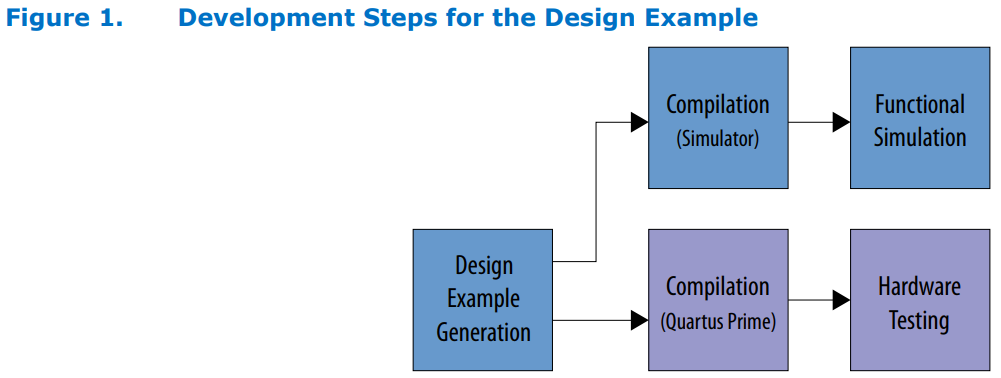

Directory Structure

Design Components for the Avalon®-MM Endpoint

Generating the Design
- Launch Platform Designer.
• If you have an existing .qsys file in your directory, the Open System dialog box appears. Click New to specify a Quartus Prime project name and custom IP variation name for your design. Then, click Create.
• If not, a new project is automatically created. Save it before moving to the next step. - In the IP Catalog, locate and select Intel Arria 10/Cyclone 10 Hard IP for PCI Express. The parameter editor appears.
- On the IP Settings tabs, specify the parameters for your IP variation.
- In the Connections panel, make the following dummy connection: rxm_bar0 to txs slave interface.
Platform Designer determines the size of the Avalon®-MM BAR master from its connection to an Avalon-MM slave device. When you generate the example design, this connection is removed. - Remove the clock_in and reset_in components that were instantiated by default.
- On the Example Design tab, the PIO design is available for your I
- For Example Design Files, select the Simulation and Synthesis
- For Generated HDL Format, only Verilog i
- For Target Development Kit, select the Intel Arria 10 GX FPGA Development Kit Currently, there is no option to select an Intel Cyclone 10 GX Development Kit when generating an example design
- Click Generate Example Design. The software generates all files necessary to run simulations and hardware tests on the Intel Arria 10 FPGA Development Kit.
Simulating the Design

- Change to the testbench simulation directory.
- Run the simulation script for the simulator of your choice. Refer to the table below.
- Analyze the results.
Table 1. Steps to Run Simulation
| Simulator | Working Directory | Instructions |
| ModelSim* | <example_design>/ pcie_example_design_tb/ pcie_example_design_tb/sim/mentor/ |
|
| VCS* | <example_design>/ pcie_example_design_tb/ pcie_example_design_tb/sim/ synopsys/vcs |
|
| NCSim* | <example_design>/ pcie_example_design_tb/ pcie_example_design_tb/sim/cadence |
|
| Xcelium* Parallel Simulator | <example_design>/ pcie_example_design_tb/ pcie_example_design_tb/sim/xcelium |
|

Compiling and Testing the Design in Hardware


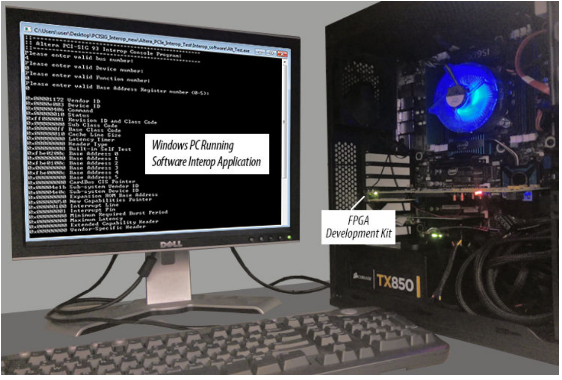
The software application to test the PCI Express Design Example on the Intel Arria 10 GX FPGA Development Kit is available on both 32- and 64-bit Windows 7 platforms. This program performs the following tasks:
- Prints the Configuration Space, lane rate, and lane width.
- Writes 0x00000000 to the specified BAR at offset 0x00000000 to initialize the memory and read it back.
- Writes 0xABCD1234 at offset 0x00000000 of the specified BAR. Reads it back and compares.
If successful, the test program displays the message ‘PASSED’
Follow these steps to compile the design example in the Quartus Prime software:
- Launch the Quartus Prime software and open the pcie_example_design.qpf file for the example design created above.
- On the Processing > menu, select Start Compilation.
The timing constraints for the design example and the design components are automatically loaded during compilation.
Follow these steps to test the design example in hardware:
- In the /software/windows/interop directory, unzip Altera_PCIe_Interop_Test.zip.
Note: You can also refer to readme_Altera_PCIe_interop_Test.txt file in this same directory for instructions on running the hardware test. - Install the Intel FPGA Windows Demo Driver for PCIe on the Windows host machine, using altera_pcie_win_driver.inf.
Note: If you modified the default Vendor ID (0x1172) or Device ID (0x0000) specified in the component parameter editor GUI, you must also modify them in altera_pcie_win_driver.inf.
a. In the <example_design> directory, launch the Quartus Prime software and compile the design (Processing > Start Compilation).
b. Connect the development board to the host
c. Configure the FPGA on the development board using the generated .sof file (Tools > Programmer).
d. Open the Windows Device Manager and scan for hardware
e. Select the Intel FPGA listed as an unknown PCI device and point to the appropriate 32- or 64-bit driver (inf) in the Windows_driver directory.
f. After the driver loads successfully, a new device named Altera PCI API Device appears in the Windows Device
g. Determine the bus, device, and function number for the Altera PCI API Device listed in the Windows Device
i. Expand the tab, Altera PCI API Driver under the
ii. Right click on Altera PCI API Device and select Properties.
iii.Note the bus, device, and function number for the device. The following figure shows one example - In the /software/windows/interop/ Altera_PCIe_Interop_Test/Interop_software directory, click Alt_Test.exe.
- When prompted, type the bus, device, and function numbers and select the BAR number (0-5) you specified when parameterizing the IP core. Note: The bus, device, and function numbers for your hardware setup may be different.
- The test displays the message, PASSED, if the test is successful.

Note: For more details on additional design implementation steps such as making pin assignments and adding timing constraints, refer to the Design Implementation chapter.
Related Information
Intel Arria 10 GX FPGA Development Kit
Design Example Description
Creating a Signal Tap Debug File to Match Your Design Hierarchy
For Intel Arria 10 and Intel Cyclone 10 GX devices, the Intel Quartus Prime software generates two files, build_stp.tcl and .xml. You can use these files to generate a Signal Tap file with probe points matching your design hierarchy.
The Intel Quartus Prime software stores these files in the / synth/debug/stp/ directory.
Synthesize your design using the Intel Quartus Prime software.
- To open the Tcl console, click View ➤ Utility Windows ➤ Tcl Console.
- Type the following command in the Tcl console: source <IP core directory>/synth/debug/stp/build_stp.tcl
- To generate the STP file, type the following command: main -stp_file <output stp file name>.stp -xml_file <input xml_file name>.xml -mode build
- To add this Signal Tap file (.stp) to your project, select Project ➤ Add/Remove Files in Project. Then, compile your
- To program the FPGA, click Tools ➤ Programmer.
- To start the Signal Tap Logic Analyzer, click Quartus Prime ➤ Tools ➤ Signal Tap Logic Analyzer.
The software generation script may not assign the Signal Tap acquisition clock in <output stp file name>.stp. Consequently, the Intel Quartus Prime software automatically creates a clock pin called auto_stp_external_clock. You may need to manually substitute the appropriate clock signal as the Signal Tap sampling clock for each STP instanc - Recompile yo
- To observe the state of your IP core, click Run Analysis.
You may see signals or Signal Tap instances that are red, indicating they are not available in your design. In most cases, you can safely ignore these signals and instances. They are present because software generates wider buses and some instances that your design does not include.
Intel Arria 10 Development Kit Conduit Interface
The Intel Arria 10 Development Kit conduit interface signals are optional signals that allow you to connect your design to the Intel Arria 10 FPGA Development Kit. Enable this interface by selecting Enable Intel Arria 10 FPGA Development Kit connection on the Configuration, Debug, and Extension Options tab of the component GUI. The devkit_status output port includes signals useful for debugging.
Table 2. The Intel Arria 10 Development Kit Conduit Interface
| Signal Name | Direction | Description |
| devkit_status[255:0] | Output | The devkit_status[255:0] bus comprises the following status signals :
|
| devkit_ctrl[255:0] | Input | The devkit_ctrl[255:0] bus comprises the following status signals. You can optionally connect these pins to an on-board switch for PCI-SIG compliance testing, such as bypass compliance testing.
|
A. Document Revision History for Intel Arria 10 and Intel Cyclone 10 GX Avalon Memory-mapped Hard IP for PCIe Design Example User Guide
| Date | Version | Changes Made |
| 2022.01.13 | 17.1 | Added clarification that the software application to test the design example is available on Windows 7 platforms. |
| 2017.11.06 | 17.1 | Made the following changes:
|
| 2017.03.15 | 16.1.1 | Rebranded as Intel. |
| 2016.10.31 | 16.1 | Initial release. |
