LG PWFSA3 Wi-Fi Bluetooth Combo Module User Manual

Model Name: PWSAF3 (Voice Recognition)

Introduction
PWFSA3 is a Wi-Fi / BLE Combo module compliant with IEEE802.11b/g/n.
The RF Module is from Murata, part number Type 1DX. (Core chipset: Cypress CYW4343W)
Features
- ARM Cortex-A7 32bit RISC Processor
- IEEE 802.11b/g/n 1X1 2.4GHz (up to 65Mbps)
- Bluetooth 5.1 LE
- Security: WEP, WPA, WPA2, WMM, WMM-PS, WMM-SA, WAPI, AES, TKIP, CKIP
- UART / SPI Interface
- Application: Home Appliance
- Supply Voltage: DC 5 V or DC 12 V
- MIC Spec. : 2Ch. Analog MEMS MIC
- SPK. Spec. : 2.0W / 4Ω
- PCB Size : 60mm x 40mm
Block Diagram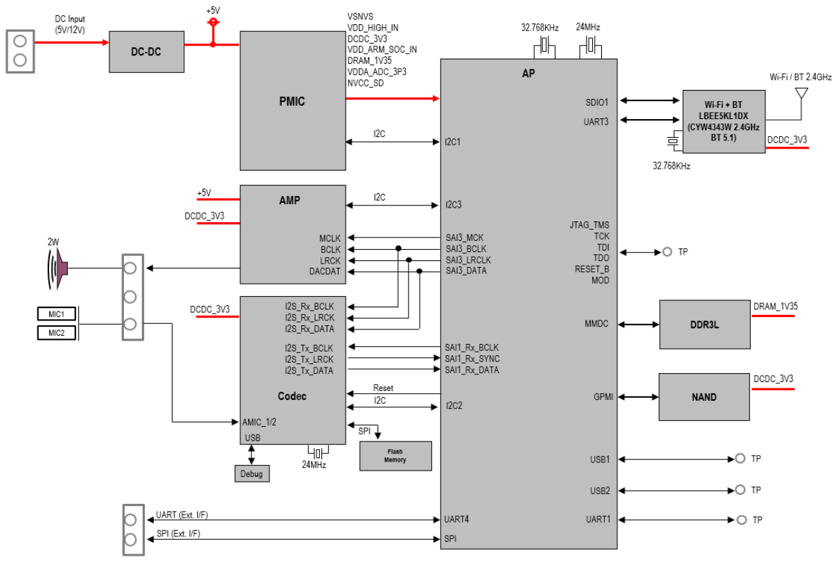

Operating Test Conditions
| Rating | Min. | Typ. | Max. | Unit |
| Supply Voltage | 5. | 5.0 | 6. | V |
| 11. | 12.0 | 13. | ||
| Operating Temperature | 0 | +25 | +70 | °C |
Electrical Characteristics
DC/RF Characteristics for IEEE802.11b (11Mbps mode)
| Specification | IEEE802.11b | |||
| Mode | DSSS / CCK | |||
| Frequency | 2400 — 2483.5MHz | |||
| Data rate | 1,2,5.5,11Mbps | |||
| Tx Characteristics | Min. | Typ. | Max. | Unit |
| DC current | ||||
| 1)Tx mode | 320 | 370 | mA | |
| 2)Rx mode | 47 | 60 | mA | |
| Output Power | 16 | 17 | 18 | dBm |
| Spectrum Mask | ||||
| 1)1st side lobes | – | -43 | -30 | dBr |
| 2)2nd side lobes | – | -54 | -50 | dBr |
| Power on and down ramp | – | 2.0 | uses | |
| RF Carrier Suppression | 15 | – | dB | |
| Modulation Accuracy (EVM) | 15 | 35 | ||
| Rx Characteristics | Min. | Typ. | Max. | Unit |
| Minimum Input Level (FER<W0) | -89 | -76 | dBm | |
| Maximum Input Level (FER<3%) | -10 | – | dBm | |
| Adjacent Channel Rejection (FER<W0) | 35 | – | – | dB |
DC/RF Characteristics for IEEE802.11g (54Mbps mode)
| Specification | IEEE802.11g | |||
| Mode | OFDM | |||
| Frequency | 2400 – 2483.5MHz | |||
| Data rate | 6,9,12,18,24,36,48,54Mbps | |||
| Tx Characteristics | Min. | Typ. | Max. | Unit |
| DC current | ||||
| 1)Tx mode | 270 | 310 | mA | |
| 2)Rx mode | 47 | 60 | mA | |
| Output Power | 12 | 13 | 14 | dBm |
| Spectrum Mask | ||||
| 1)9MHz to 11 MHz (OdB – -20dB) | -33 | -20 | dBr | |
| 2)11MHz to 20MHz (-20dB – -28dB) | -41 | -28 | dBr | |
| 3)20MHz to 30MHz (-28dB – -40dB) | -53 | -40 | dBr | |
| 4)30MHz to 33MHz (-40dB) | -53 | -40 | dBr | |
| Constellation Error (EVM) | – | -30 | -25 | dB |
| Rx Characteristics | Min. | Typ. | Max. | Unit |
| Minimum Input Level (PER510%) | – | -75 | -65 | dBm |
| Maximum Input Level (PER510°/0) | -20 | – | – | dBm |
| Adjacent Channel Rejection (PER510%) | -1 | – | – | dB |
DC/RF Characteristics for IEEE802.11n (65Mbps mode)
| Specification | IEEE802.11n | |||
| Mode | OFDM | |||
| Frequency | 2400 — 2483.5MHz | |||
| Data rate | 6.5,13,19.5,26,39,52,58.5,65Mbps | |||
| Tx Characteristics | Min. | Typ. | Max. | Unit |
| DC current | ||||
| 1)Tx mode | 260 | 300 | mA | |
| 2)Rx mode | 47 | 60 | mA | |
| Output Power | 12 | 13 | 14 | dBm |
| Spectrum Mask | ||||
| 1)9MHz to 11 MHz (OdB — -20dB) | -33 | -20 | dBr | |
| 2)11 MHz to 20MHz (-20dB — -28dB) | -41 | -28 | dBr | |
| 3)20MHz to 30MHz (-28dB — -40dB) | -53 | -45 | dBr | |
| 4)30MHz to 33MHz (-40dB) | -53 | -45 | dBr | |
| Constellation Error (EVM) | -31 | -27 | dB | |
| Rx Characteristics | Min. | Typ. | Max. | Unit |
| Minimum Input Level (PER10%) | – | -73 | -64 | dBm |
| Maximum Input Level (PER10c/o) | -20 | – | dBm | |
| Adjacent Channel Rejection (PEIR10%) | -2 | – | dB | |
DC/RF Characteristics for Bluetooth (LE)
| Bluetooth specification (Power class) | Version 5.1 (LE) | |||
| Channel frequency (Spacing) | 2402 — 2480MHz (2MHz) | |||
| Number of RF Channel | 40 | |||
| Item / Condition | Min. | Typ. | Max. | Unit |
| Center Frequency | 2402 | 2480 | MHz | |
| Channel Spacing | 2 | MHz | ||
| Number of RF Channel | 40 | |||
| Output power | 7 | 8 | 9 | dBm |
| Modulation Characteristics | ||||
| 1)Af1avg | 225 | 275 | kHz | |
| 2)Af2max (at 99.9%) | 185 | kHz | ||
| 3)Af2avg / Af1avg | 0.8 | |||
| Carrier frequency offset and drift | ||||
| 1)Frequency offset | 150 | kHz | ||
| 2)Frequency drift | 50 | kHz | ||
| 3)Drift rate | 20 | kHz | ||
| Receiver sensitivity (PER < 30.8%) | -95 | -70 | dBm | |
| Maximum input signal level (PER < 30.8%) | -10 | dBm | ||
| PER Report Integrity | 50 | 65. | ||
PIN MAP
PCB View

CN101
| Pin No. | Name | I/O | Description |
| 1 | VDD | I | VDD 5.0V, 12V |
| 2 | GND | – | Ground |
CN102
| Pin No. | Name | I/O | Description |
| 1 | GND | – | Ground |
| 2 | EXT_SPI_WAKE UP | 0 | SPI Slave wake up |
| 3 | EXT_SPI_STATUS | I | Request data transaction in Slave device |
| 4 | EXT_SPI_CS | 0 | SPI Slave Chip Select |
| 5 | EXT_SPI_CLK | 0 | SPI Clock |
| 6 | EXT_SPI_MOSI | 0 | SPI Master Output Slave Input |
| 7 | EXT_SPI_MISO | I | SPI Master Input Slave Output |
| 8 | GND | – | Ground |
| 9 | UART_TX | 0 | UART Communication signal line |
| 10 | UART_RX | I | UART Communication signal line |
CN103
| Pin No. | Name | I/O | Description |
| 1 | MIC2_BIAS | 0 | MIC2 bias output |
| 2 | MIC2_N | I | MIC2 negative input |
| 3 | MIC2_P | I | MIC2 positive input |
| 4 | MICLBIAS | 0 | MIC1 bias output |
| 5 | MICLN | I | MIC1 negative input |
| 6 | MICLP | I | MIC1 positive input |
| 7 | SPK_N | 0 | Negative speaker output |
| 8 | SPK_P | 0 | Positive speaker output |
FCC, ISED Statement
FCC Part 15.19
This device complies with part 15 of the FCC Rules.
Operation is subject to the following two conditions: (1) This device may not cause harmful interference, and (2) this device must accept any interference received, including interference that may cause undesired operation.
FCC Part 15.21
Any changes or modifications (including the antennas) to this device that are not expressly approved by the manufacturer may void the user’s authority to operate the equipment.
FCC Part 15.247
This device complies with part 15.247 of the FCC Rules.
FCC RF Radiation Exposure Statement: This equipment complies with FCC RF Radiation exposure limits set forth for an uncontrolled environment.
This device and its antenna must not be co-located or operating in conjunction with any other antenna or transmitter.
This equipment should be installed and operated with a minimum distance of 20 cm between the radiator and your body.
Please notice that if the FCC identification number is not visible when the module is installed inside another device, then the outside of the device into which the module is installed must also display a label referring to the enclosed module.
This exterior label can use wording such as the following: “Contains FCC ID: BEJ-PWFSA3” any similar wording that expresses the same meaning may be used.
Manual Information to the End User
The module is limited to OEM installation ONLY.
The OEM integrator is responsible for ensuring that the end-user has no manual instruction to remove or install-module.
The module is limited to installation in the fixed application;
Separate approval is required for all other operating configurations, including portable configurations with respect to Part 2.1093 and different antenna configurations.
There is a requirement that the grantee provides guidance to the host manufacturer for compliance with Part 15B requirements.
This device contains license-exempt transmitter(s)/receiver(s) that comply with Innovation, Science, and Economic Development Canada’s license-exempt RSS(s).
Operation is subject to the following two conditions:
(1) This device may not cause interference.
(2) This device must accept any interference, including interference that may cause undesired operation of the device.
IC RF Radiation Exposure Statement: This equipment complies with IC RF Radiation exposure limits set forth for an uncontrolled environment. This device and its antenna must not be co-located or operating in conjunction with any other antenna or transmitter.
This equipment should be installed and operated with a minimum distance of 20 cm between the radiator and your body.
Please notice that if the IC identification number is not visible when the module is installed inside another device, then the outside of the device into which the module is installed must also display a label referring to the enclosed module.
This exterior label can use wording such as the following: “Contains IC:2703N-PWFSA3” any similar wording that expresses the same meaning may be used.
Integration instruction
The OEM integrator has to be aware not to provide information to the end-user regarding how to install or remove this RF module in the user’s manual of the end product which integrates this
module. The end-user manual shall include all required regulatory information/warning as shown in this manual.
For mobile and fixed operation configurations the antenna gain, including cable loss will be registered under the following identifiers:
FCC Identifier: BEJ-PWFSA3
Industry Canada Certification Number: 2703N-PWFSA3
Granted to LG Electronics USA / LG Electronics Inc.
The final host product still requires Part 15 Subpart B compliance testing with the modular transmitter installed.