Intel FPGA Download Cable II Plug Connection User Guide


intel FPGA Download Cable II Plug Connection

Setting Up the Intel® FPGA Download Cable II
Attention: The download cable name has changed to Intel® FPGA Download Cable II . Some file names may still refer to USB-Blaster II.
Attention: Unless otherwise stated, any usage of the terms ‘cable’ or ‘download cable’ shall specifically refer to the Intel FPGA Download Cable II.
The Intel FPGA Download Cable II interfaces a USB port on a host computer to an Intel FPGA mounted on a printed circuit board. The Intel FPGA Download Cable II sends data from the host PC to a standard 10-pin header connected to the FPGA. You can use the Intel FPGA Download Cable II for the following:
- Iteratively download configuration data to a system during prototyping
- Program data into the system during production
- Advanced Encryption Standard (AES) key and fuse programming
Supported Devices and Systems
You can use the Intel FPGA Download Cable II to download configuration data to the following devices:
- Intel Stratix® series FPGAs
- Intel Cyclone® series FPGAs
- Intel MAX® series CPLDs
- Intel Arria® series FPGAs
You can perform in-system programming of the following devices:
- EPC4, EPC8, and EPC16 enhanced configuration devices
- EPCS1, EPCS4, EPCS16, EPCS64, and EPCS/Q128, EPCQ256, EPCQ-L and EPCQ512 serial configuration devices
The Intel FPGA Download Cable II supports target systems using the following:
- 5.0-V TTL, 3.3-V LVTTL/LVCMOS
- Single-ended I/O standards from 1.5 V to 3.3 V
Power Source Requirements
- 5.0 V from the Intel FPGA Download Cable II
- Between 1.5 V and 5.0 V from the target circuit board
Software Requirements and Support
- Windows 7/8/10 (32-bit and 64-bit)
- Windows XP (32-bit and 64-bit)
- Windows Server 2008 R2 (64-bit)
- Linux platforms such as Red Hat Enterprise 5
Note:
Use the Intel Quartus® Prime software version 14.0 or later to configure your device. Intel Quartus Prime version 13.1 supports most of the Intel FPGA Download Cable II’s capabilities. If you use this version, install the latest patch for full compatibility. The Intel FPGA Download Cable II also supports the following tools:
- Intel Quartus Prime Programmer (and stand-alone version)
- Intel Quartus Prime Signal Tap II Logic Analyzer (and stand-alone version)
- JTAG and debug tools supported by the JTAG Server. For example:
- System Console
- Nios® II debugger
- Arm* DS-5 debugger
Installing the Intel FPGA Download Cable II for Configuration or Programming
- Disconnect the power cable from the circuit board.
- Connect the Intel FPGA Download Cable II to the USB port on your computer and to the download cable port.
- Connect the Intel FPGA Download Cable II to the 10-pin header on the device board.
- Reconnect the power cable to reapply power to the circuit board.
The Intel FPGA Download Cable II

Note:
For plug and header dimensions, pin names, and operating conditions, see the Intel FPGA Download Cable II Specifications chapter.
Related Information
Intel FPGA Download Cable II Specifications on page 8
Installing the Intel FPGA Download Cable II Driver on Windows 7/8/10 Systems
You must have system administration (administrator) privileges to install the download cable drivers. The download cable drivers are included in the Intel Quartus Prime software installation. Before you begin the installation, verify that the download cable driver is located in your directory: \<Quartus Prime system directory>\drivers\usb-blaster-ii.
- Connect the download cable to your computer’s USB port. When plugged in for the first time, a message appears stating Device driver software was not successfully installed.
- From the Windows Device Manager, locate Other devices and right-click the top USB-BlasterII.
You need to install drivers for each interface: one for the JTAG interface and one for the System Console interface. - On the right-click menu, click Update Driver Software. The Update Driver Software – USB BlasterII dialog appears. 1. Setting Up the Intel® FPGA Download Cable II 683719 | 2019.10.23 Send
- Click Browse my computer for driver software to continue.
- Click Browse… and browse to the location of the driver on your system: \<Quartus Prime system directory>\drivers\usb-blaster-ii. Click OK.
- Click Next to install the driver.
- Click Install when asked if you want to install. You should now have a JTAG cable showing in the Device Manager.
- Now, install the driver for the other interface. Go back to step 2 and repeat the process for the other download cable devices. When you are finished, you will have added USB-Blaster II (JTAG interface) under JTAG cables.


Installing the Intel FPGA Download Cable II Driver on Linux Systems
For Linux, the download cable supports Red Hat Enterprise 5, 6, and 7. To access the cable, the Intel Quartus Prime software uses the built-in Red Hat USB drivers, the USB file system (usbfs). By default, root is the only user allowed to use usbfs. You must have system administration (root) privileges to configure the Intel FPGA Download Cable II drivers.
- Create a file named /etc/udev/rules.d/51-usbblaster.rules and add the following lines to it. (The .rules file may already exist if you have installed an earlier version.)
- Red Hat Enterprise 5 and above Intel FPGA Download Cable II
SUBSYSTEMS==”usb”, ATTRS{idVendor}==”09fb”, ATTRS{idProduct}==”6010″, MODE=”0666″
SUBSYSTEMS==”usb”, ATTRS{idVendor}==”09fb”, ATTRS{idProduct}==”6810″, MODE=”0666″
Caution: There should be only three lines in this file, one starting with a comment and two starting with BUS. Do not add extra line breaks to the .rules file.
- Red Hat Enterprise 5 and above Intel FPGA Download Cable II
- Complete your installation by setting up the programming hardware in the Intel Quartus Prime software. Go to the “Setting Up the Intel FPGA Download Cable II Hardware with the Intel Quartus Prime Software” section.
For more information about download cable driver installation, refer to the Cable and Adapter Drivers Information page.
Related Information
- Setting Up the Intel FPGA Download Cable II Hardware with the Intel Quartus Prime Software on page 7
- Cable and Adapter Drivers Information
Installing the Intel FPGA Download Cable II Driver on Windows XP Systems
You must have system administration (administrator) privileges to install the download cable driver. The download cable drivers are included in the Intel Quartus Prime software installation. Before you begin the installation, verify that the download cable driver is located in your directory: \<Quartus Prime system directory>\drivers\usb-blasterii.
Setting Up the Intel FPGA Download Cable II Hardware with the Intel Quartus Prime Software
- Start the Intel Quartus Prime software.
- From the Tools menu, click Programmer.
- Click Hardware Setup.
- Click the Hardware Settings tab.
- From the Currently selected hardware list, select Intel FPGA Download Cable II.
- Click Close.
- In the Mode list, choose an appropriate programming mode. The table below describes each mode.
Programming Modes
| Mode | Mode Description |
| Joint Test Action Group (JTAG) | Programs or configures all devices supported by Quartus Prime software via JTAG programming. |
| In-Socket Programming | Not supported by the Intel FPGA Download Cable II. |
| Passive Serial Programming | Configures all devices supported by Quartus Prime software excluding enhanced configuration devices (EPC) and serial configuration devices (EPCS/Q). |
| Active Serial Programming | Programs a single EPCS1, EPCS4, EPCS16, EPCS64, EPCS/ Q128, EPCQ256, EPCQ-L and EPCQ512 device. |
For detailed help on using the Quartus Prime Programmer, refer to the Intel Quartus Prime Pro Edition User Guide: Programmer or the Intel Quartus Prime Standard Edition User Guide: Programmer.
Related Information
- Intel Quartus Prime Pro Edition User Guide: Programmer
- Intel Quartus Prime Standard Edition User Guide: Programmer
Intel FPGA Download Cable II Specifications
Voltage Requirements
The Intel FPGA Download Cable II VCC(TRGT) pin must be connected to a specific voltage for the device being programmed. Connect pull-up resistors to the same power supply as the Intel FPGA Download Cable II : VCC(TRGT).
Intel FPGA Download Cable II VCC(TRGT) Pin Voltage Requirements
| Device Family | Intel FPGA Download Cable II VCC Voltage Required |
| Arria GX | As specified by VCCSEL |
| Arria II GX | As specified by VCCPD or VCCIO of Bank 8C |
| Arria V | As specified by VCCPD Bank 3A |
| Intel Arria 10 | As specified by VCCPGM or VCCIO |
| Cyclone III | As specified by VCCA or VCCIO |
| Cyclone IV | As specified by VCCIO. Bank 9 for Cyclone IV GX and Bank 1 for Cyclone IV E devices. |
| Cyclone V | As specified by VCCPD Bank 3A |
| EPC4, EPC8, EPC16 | 3.3 V |
| EPCS1, EPCS4, EPCS16, EPCS64, EPCS128 | 3.3 V |
| EPCS/Q16, EPCS/Q64, EPCS/Q128, EPCQ256, EPCQ512 | 3.3 V |
| EPCQ-L | 1.8 V |
| MAX II, MAX V | As specified by VCCIO of Bank 1 |
| Intel MAX 10 | As specified by VCCIO |
| Stratix II, Stratix II GX | As specified by VCCSEL |
| Stratix III, Stratix IV | As specified by VCCPGM or VCCPD |
| Stratix V | As specified by VCCPD Bank 3A |
Cable-to-Board Connection
A standard USB cable connects to the USB port on the device.
Intel FPGA Download Cable II Block Diagram

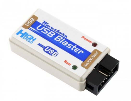
Intel FPGA Download Cable II Plug Connection
The 10-pin female plug connects to a 10-pin male header on the circuit board containing the target device.
Intel FPGA Download Cable II 10-Pin Female Plug Dimensions – Inches & Millimeters

Intel FPGA Download Cable II Dimension – Inches and Millimeters

| Pin | Active Serial (AS) Mode | Passive Serial (PS) Mode | JTAG Mode | |||
| Signal Name | Description | Signal Name | Description | Signal Name | Description | |
| 1 | DCLK | Configuration Clock | DCLK | Configuration Clock | TCK | Test Clock |
| 2 | GND | Signal ground | GND | Signal ground | GND | Signal ground |
| 3 | CONF_DONE | Configuration done | CONF_DONE | Configuration done | TDO | Test Data Output |
| 4 | VCC(TRGT) | Target power supply | VCC(TRGT) | Target power supply | VCC(TRGT) | Target power supply |
| 5 | nCONFIG | Configuration control | nCONFIG | Configuration control | TMS | Test Mode Select Input |
| 6 | nCE | Target chip enable | – | – | PROC_RST | Processor Reset |
| 7 | DATAOUT | Active serial data out | nSTATUS | Configuration Status | – | – |
| 8 | nCS | Serial configuration device chip select | nCS | Serial configuration device chip select | – | – |
| 9 | ASDI | Active serial data in | DATA0 | Passive serial data in | TDI | Test Data Input |
| 10 | GND | Signal ground | GND | Signal ground | GND | Signal ground |

| Symbol | Parameter | Conditions | Min | Max | Unit |
| VCC(TRGT) | Target supply voltage | With respect to ground | –0.5 | 6.5 | V |
| VCC(USB) | USB supply voltage | With respect to ground | –0.5 | 6.0 | V |
| continued… | |||||
| Symbol | Parameter | Conditions | Min | Max | Unit |
| II | Target side input current | Pin 7 | –100.0 | 100.0 | mA |
| II(USB) | USB supply current | VBUS | – | 200.0 | mA |
| Io | Target side output current | Pins: 1, 5, 6, 8, 9 | –50.0 | 50.0 | mA |
Intel FPGA Download Cable II Recommended Operating Conditions
| Symbol | Parameter | Conditions | Min | Max | Unit |
| VCC(TRGT) | Target supply voltage, 5.0-V operation | — | 4.75 | 5.25 | V |
| Target supply voltage, 3.3-V operation | — | 3.0 | 3.6 | V | |
| Target supply voltage, 2.5-V operation | — | 2.375 | 2.625 | V | |
| Target supply voltage, 1.8-V operation | — | 1.71 | 1.89 | V | |
| Target supply voltage, 1.5-V operation | — | 1.43 | 1.57 | V |
Intel FPGA Download Cable II DC Operating Conditions
| Symbol | Parameter | Conditions | Min | Max | Unit |
| VIH | High-level input voltage | VCC(TRGT) >= 2.0 V | 0.7 x VCC(TRGT) | — | V |
| High-level input voltage | VCC(TRGT) < 2.0 V | 0.65 x VCC(TRGT) | — | V | |
| VIL | Low-level input voltage | VCC(TRGT) >= 2.0 V | — | 0.3 x VCC(TRG T) |
V |
| Low-level input voltage | VCC(TRGT) >= 2.0 V | — | 0.2 x VCC(TRG T) |
V | |
| VOH | 5.0-V high-level output voltage | VCC(TRGT) = 4.5 V, IOH = -32 mA | 3.8 | — | V |
| 3.3-V high-level output voltage | VCC(TRGT) = 3.0 V, IOH = -24 mA | 2.4 | — | V | |
| 2.5-V high-level output voltage | VCC(TRGT) = 2.3 V, IOH = -12 mA | 1.9 | — | V | |
| 1.8-V high-level output voltage | VCC(TRGT) = 1.65 V, IOH = -8 mA | 1.2 | — | V | |
| 1.5-V high-level output voltage | VCC(TRGT) = 1.4 V, IOH = -6 mA | 1.0 | — | V | |
| VOL | 5.0-V low-level output voltage | VCC(TRGT) = 4.5 V, IOL = 32 mA | — | 0.55 | V |
| 3.3-V low-level output voltage | VCC(TRGT) = 3.0 V, IOL = 24 mA | — | 0.55 | V | |
| 2.5-V low-level output voltage | VCC(TRGT) = 2.3 V, IOL = 12mA | — | 0.3 | V | |
| 1.8-V low-level output voltage | VCC(TRGT) = 1.65 V, IOL = 8mA | — | 0.45 | V | |
| 1.5-V low-level output voltage | VCC(TRGT) = 1.4 V, IOL = 6mA | — | 0.3 | V | |
| ICC(TRGT) | Operating current (No Load) | VCC(TRGT)=5.5 V | — | 316 | uA |
JTAG Timing Constraints and Waveforms
Timing Waveform for JTAG Signals (From Target Device Perspective)

JTAG Timing Constraints for the Target Device
| Symbol | Parameter | Min | Max | Unit |
| tJCP | TCK clock period | 41.67 | — | ns |
| tJCH | TCK clock high time | 20.83 | — | ns |
| tJCL | TCK clock low time | 20.83 | — | ns |
| tJPCO | JTAG port clock to JTAG Header output | — | 5.46 (2.5 V) 2.66 (1.5 V) |
ns |
| continued… | ||||
| Symbol | Parameter | Min | Max | Unit |
| tJPSU_TDI | JTAG port setup time (TDI) | — | 24.42 | ns |
| tJPSU_TMS | JTAG port setup time (TMS) | — | 26.43 | ns |
| tJPH | JTAG port hold time | — | 17.25 | ns |
The simulated timing is based on a slow timing model, which is a worst-case scenario environment. For device-specific JTAG timing information, refer to the related device data sheet.
Intel FPGA Download Cable II Timing Constraints

- Changing the TCK Frequency on page 14
- Documentation: Data Sheets
Changing the TCK Frequency
The Intel FPGA Download Cable II has a default TCK frequency of 24 MHz. Where signal integrity and timing prevent operating at 24 MHz, change the TCK frequency of the download cable:
- Open the command line interface with the Intel Quartus Prime bin directory in your path (for example, C:\<Intel Quartus Prime installed folder> \<Intel Quartus Prime version>\quartus\bin64).
- Type the following command to change the TCK frequency:
- <cable number> is the download cable to be modified.
- <frequency> is the desired TCK frequency. Use one the following supported rates:
- 4 MHz
- 16 MHz
- 6 MHz
- 24/n MHz (between 10 KHz and 6 MHz, where n represents an integer value number)
- <unit prefix> is the unit prefix for the frequency (e.g. M for MHz).
TCK Frequency Auto-Adjust for Intel FPGA Download Cable II
The TCK Frequency Auto-Adjust is a new feature implemented in the Intel Quartus Prime 19.1 Pro release for the Intel FPGA Download Cable II . This feature provides convenience and prevents incorrect TCK frequency setting that might cause slower device failure during JTAG operation. The auto-adjust feature is enabled as default. To disable the auto-adjust feature, you can use the command line interface or Programmer GUI. The status of the feature is reset to default (enabled) when the cable is reconnected or the JTAG server is restarted. The auto-adjust feature always applies optimum frequency that can support on the current JTAG chain based on the BYPASS tests. If you specified a TCK frequency, the auto-adjust feature stops at the specified TCK frequency with the condition that the BYPASS tests are passing at the frequency. Otherwise, the auto-adjust feature continues and will stop at a lower frequency which the BYPASS tests are passing. This new feature is only applicable when both Intel Quartus Prime and the JTAG server are in version 19.1. If you use Intel Quartus Prime 19.1 with an older JTAG server (before version 19.1), the auto-adjust feature is not available.
Note: The TCK frequency auto-adjust is designed based on the hard JTAG scan chain. For the virtual JTAG scan chain, the TCK frequency after auto-adjust may still require further adjustment from the user for successful JTAG operation.
Programmer GUI
A checkbox is added in the Programmer’s “Hardware Setup” dialog box to turn On/Off the frequency adjust feature. The checkbox is enabled when the frequency auto-adjust feature is available . Otherwise, it is greyed out. If the frequency auto adjusts feature is enabled, a new adjusted TCK frequency value will be shown under the message box of the programmer GUI.
Programmer GUI (Hardware Settings → Hardware Settings Tab)

Additional Information
- Incorrect Windows settings or some unknown problem with the Intel FPGA Download Cable II driver
- The version of JTAG-related software like Jtagconfig or Jtagserver not match the version of Intel Quartus Prime software
- The version of the Intel FPGA Download Cable II driver is old, not proper, or corrupted
- Open a command prompt of Windows OS
- Execute the following command:
- If the version in the message does not match the Intel Quartus Prime version that you use, you must modify the user system variables for your Windows account or the system variables.
- Go to <Quartus Prime software install folder>\quartus\bin64 for Intel Quartus Prime. Go to <Quartus Prime Programmer install folder> \qprogrammer\bin64 or <Quartus Prime Programmer install directory>\qprogrammer\quartus\bin64 for Intel Quartus Prime Programmer tool.
- Execute the following command: qreg.exe –force –jtag –setqdir
- Intel recommends you verify the environment variables using the manual setting procedure explained in the section below.
Manual Setting
- Open Environment Variables window of Windows OS Windows Settings > Type “Environment” into the search area > Choose Edit the system environment variables
- Check if Path variable has %QUARTUS_ROOTDIR%\bin64 in System variables or User variables for your account. If not present, add %QUARTUS_ROOTDIR%\bin64
- Check if QUARTUS_ROOTDIR variable is in a right path that bin64 folder locates Directory for Intel Quartus Prime: <Quartus Prime software install folder>\quartus Directory for Intel Quartus Prime Programmer tool: < Quartus Prime Programmer install folder>\qprogrammer or < Quartus Prime Programmer install directory>\qprogrammer\quartus
- If you notice these variables in both System variables or User variables for your account, Intel recommends that one of them should be deleted.
- Restart your computer and check the version of jtagconfig using step 1 and 2
Jtagserver Setting
- Open Windows OS command prompt
- Execute the following command: jtagconfig –serverinfo The example output message is Installed JTAG server is ‘<Quartus Prime install folder>\quartus \bin64\jtagserver.exe’ Service manager reports server is running Server reports path: <Quartus Prime install folder>\quartus \bin64\jtagserver.exe Server reports version: Version 18.1.1 Build 646 04/11/2019 SJ Standard Edition Remote clients are disabled (no password)
- Set the environment variables correctly following the steps described in the jtagconfig version setting in the sections above.
- Execute the following commands
- Restart your computer
Install/Reinstall the Intel FPGA Download Cable II driver
- Connect your Intel FPGA Download Cable or Intel FPGA Download Cable II
- Open Device Manager window of Windows OS Windows Settings > Type “Device Manager” into the search area > Choose Device Manager
- Find Intel FPGA Download Cable II under JTAG cables or Intel FPGA Download Cable under Universal Serial Bus controllers
- Choose Intel FPGA Download Cable or Intel FPGA Download Cable II
- Right click and choose Uninstall device from context menu
- Enable Delete the driver software for this device and click Uninstall
- If you see another Intel FPGA Download Cable or Intel FPGA Download Cable II, uninstall it too
- Reinstall the drivers following the steps in section Windows Troubleshooting Procedure for Intel FPGA Download Cable II on page 18
Troubleshooting Procedure for Error when scanning hardware No Devices
You might see this error when connecting multiple download cables to your computer and executing jtagconfig command. Error when scanning hardware – No devices It takes a certain finite amount of time for your computer to finish the USB device enumeration after connecting USB devices. The more USB devices are connected, the more time is required for the USB device enumeration. The above error occurs when jtagconfig command is executed before your computer finishes the USB device enumeration to recognize all download cables connected. The error seems to occur only when jtagconfig command is executed right after multiple download cables are connected
Troubleshooting Procedure
You need to wait for a while until your computer finishes the USB device enumeration after your Intel FPGA Download Cable II is connected. You can use Device Manager on Windows or lsusb command on Linux to check if your Intel FPGA Download Cable II is recognized on your computer. For Windows: Open Device Manager and check if Intel FPGA Download Cable II (JTAG interface) under JTAG cables or Intel FPGA Download Cable under Universal Serial Bus controller is listed. For Linux: Open a command shell, type lsusb, and check if the device with ID of 09fb:6001, 09fb:6002, 09fb:6003, 09fb:6010, or 09fb:6810 is listed.
Certification Statements
RoHS Compliance
The table below lists hazardous substances included with the Intel FPGA Download Cable II. A value of 0 indicates that the concentration of the hazardous substance in all homogeneous materials in the parts is below the relevant threshold as specified by the SJ/T11363-2006 standard.
Hazardous Substances and Concentration
| Part Name | Lead (Pb) | Cadmium (Cd) | Hexavelent Chromium (Cr6+) | Mercury (Hg) | Polybrominate d biphenyls (PBB) | Polybrominate d diphenyl Ethers (PBDE) |
| Electronic Components | 0 | 0 | 0 | 0 | 0 | 0 |
| Populated Circuit Board | 0 | 0 | 0 | 0 | 0 | 0 |
| Manufacturing Process | 0 | 0 | 0 | 0 | 0 | 0 |
| Packing | 0 | 0 | 0 | 0 | 0 | 0 |
USB 2.0 Certification
This product is USB 2.0 certified.
CE EMI Conformity Caution
This product is delivered conforming to relevant standards mandated by Directive 2004/108/EC. Because of the nature of programmable logic devices, it is possible for the user of this product to modify it in such a way as to generate electromagnetic interference (EMI) that exceeds the limits established for this equipment. Any EMI caused as the result of modifications to the delivered material is the sole responsibility of the user. A. Additional Information 683719 | 2019.10.23 Intel
Revision History
Revision History of the Intel FPGA Download Cable II User Guide
| Document Version | Changes |
| 2019.10.23 | Added the following sections: • Windows Troubleshooting Procedure for Intel FPGA Download Cable II on page 18 • Troubleshooting Procedure for Error when scanning hardware – No Devices on page 20 |
| 2019.04.01 | Added new chapter TCK Frequency Auto-Adjust for Intel FPGA Download Cable II |
| 2018.04.19 | Updated 10-Pin Female Plug Signal Names and Programming Modes on page 10 |
Revision History of the Intel FPGA Download Cable II User Guide
| Date | Version | Changes |
| October 2016 | 2016.10.28 | The name USB-Blaster II has changed to Intel FPGA Download Cable II. |
| December 2015 | 2015.12.11 | Updated Sections: • Supported Devices and Systems • Setting Up the USB-Blaster II Hardware with the Quartus II Software • Voltage Requirements • 10-Pin Female Plug Signal Names and Programming Modes |
| September 2014 | 1.2 | • Added that the USB-II download cable supports Advanced Encryption Standard (AES) key and fuse programming. • Added magenta LED color to Figure 1-1 supporting multiple cable use. • Clarified a cross reference pointing to device-specific JTAG timing information. |
| June 2014 | 1.1 | • Added LED color table to Figure 1-1. • Added “JTAG Timing Constraints and Waveforms” section. • Added “Changing the TCK Frequency” section. |
| January 2014 | 1.0 | Initial release. |